TFP is now offering a new coating process, Molecular Vapour Deposition (MVD), that may be able to meet all of the environmental demands for circuit board protection and other surfaces.
The process could also be highly cost-effective.
This process is brand new to the electronics coating market and many other industrial sectors and could be a viable solution for many products.
What is Molecular Vapour Deposition (MVD)?
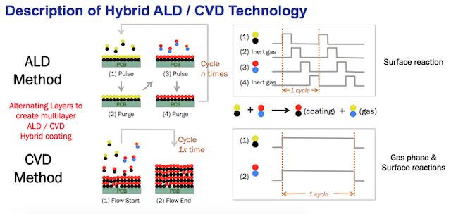
MVD is a hybrid coating technique using two different techniques, Atomic Layer Deposition (ALD) and Chemical Vapor Deposition (CVD), in combination.
This hybrid process uses multiple layers of ultra-thin coatings with differing properties to build a completely protective coating across the substrate of the device.
The final coating built up is much thinner than many other traditional coatings. However, its protective performance has been found to be superior to them all in most categories of testing so far.
Further, the really exciting part about this technology is the cost of processing.
Since the coating is extremely thin then it has been found that no masking is required.
This is because when components like connectors are joined together then the ultrathin coating does not prevent electrical connection. Even better, the physical protection is not compromised.
This means that the cost of process is purely the cost of application of the material and nothing else.
Since the process is relatively low cost then this does offer a very interesting alternative to the traditional coating materials.
So how is the MVD film applied to a substrate?
The film is built up of alternating layers of ALD and CVD thin coating layers.
The ALD layer is a ceramic-based material providing the insulating properties. The CVD film is an organic material that provides the barrier protection.
Once the required film thickness is achieved for the hybrid film then a final hydrophobic layer is applied that combines with the ALD and CVD layers to provide a highly effective barrier.
So how well does the MVD coating perform when protecting circuit boards?
Data was recently presented at Apex in Sand Diego that was applied to LED circuit boards.
The customer LED product was for outdoor application. For testing, the customer used in-house test methods to prove the technology.
The LED circuit was exposed to customer tests for resistance against salt, moisture and temperature.
The test methods included:
- Initial test submerged in DI water dip for 12 hours
- Second test submerged in 25% concentration saltwater dip for 17 hours
- Third test 2 x 6 hour cycles in water ramped from room temperature to 70°C
After each test the boards were tested for failure or problems.
The LED circuit passed on all tests. All results achieved were completed with no masking of components and zero light loss in LED opacity.
The electrical connections were found to be excellent and the coating did not affect the integrity of the connectors.
So, just how good is the MVD coating as a protective material?
Generally, with protective coatings for electronics then Parylene is considered the gold standard in most cases.
So, we compared Parylene with the MVD coating material.
| Property | Parylene | MVD |
| Hardness | Soft | Hard |
| Wear resistance/Handling Ease | Poor | Excellent |
| Water Vapor Transmission Rate | Good | Excellent |
| Temperature Resistance (extended time) | 100°C | 350°C |
| Color | Gray/white | Clear |
| Adhesion to various materials | Poor | Excellent |
| Scalable to large production | Poor | Excellent |
| Process Time | 8 – 12 hrs | 8 – 12 hrs |
| Hydrophobicity | Good | Good – Excellent |
| Cost | High | Low – Med |
What we also identified for the material were some key properties for LEDs.
- The Water Vapor Transmission Rate (WVTR) is superior to Parylene so the coating is far more waterproof for the LEDs
- Coating adhesion is superior as it covalently bonds to the substrate. So, the lifetime of the material will be better on the circuit.
- The hybrid coating is UV stable whereas Parylene in general is not. This is an important criteria for coatings exposed outside on LEDs
- The coating stayed 100% transparent during testing (no loss of lux). That again is important for LEDs.
- The coating thickness of the hybrid material is x10 LESS than the Parylene. This aids light transmission and electric connectivity
So, in reality the MVD material could just be what the high volume electronics industry is looking for in protecting their circuits.
Its almost certain that the coating will have other applications beyond electronics as well.
Ask us how we can help you with your thin film projects now
Talk to us about your project. See how we can save you money now.
We have the knowledge, tools, experience and the complete solutions whatever you need. We are here to help.
Contact us now.