Advanced Nano Materials
Plasma Based Coating Development, Processes and Services
A member of Thin Film Partners has developed proprietary coating methods and technology to uniformly and reproducibly apply barrier and functional conformal coatings via low temperature plasma. A broad spectrum of coating chemistries can be applied on thermoplastic, thermoset, metallic, ceramic and mixed substrates. Our solutions span the microelectronic, medical device and photovoltaic applications of surface modifications as well as, defense and homeland security applications.
Applications of interest have included:
- Semiconductor and wafer fab barrier and functional coatings.
- Circuit board moisture and organic barrier coatings.
- Medical device barrier and functional coatings.
- Reactive surface preparation for further surface treatments.
- Fuel barrier coatings.
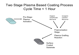
These surface modifications provide complete coverage. They are conformal to irregular surface shapes and are tightly bounded with unusually high durability by today’s standards. The first stages activate the substrate’s surface and the second is a surface graft utilizing specific organic and pre-ceramic monomers to a depth of 50-200nm.
We have used plasma based technology on a variety of polymeric and inorganic substrates to produce nano scale grafted organic and ceramic structures. The coatings platform is robust and has been demonstrated on many classes of monomers.
| Chemistry Type | Key Properties |
| Styrene | Optical clarity, low cost |
| Aliphatic Alkene | Optical clarity, uv stability, low cost, can be elastomeric, reactive and/or crosslinkable |
| Olefinic Terpenes | Natural product green origin, may be elastomeric and/or crosslinkable, low cost |
| Ceramic | Optical clarity, water and hydrocarbon barrier, uv stability, hard surface |
| Fluoroalkene | UV stability, substrate adhesion low coefficient of friction, thermal stability |
| Fluorosilyls | Hydrophobic, thermal stability, uv stability |
| Multilayer Structures | Steam autoclave barrier protection, reactive subcoats. |
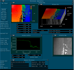
As an example, optical interferometry of a masked step edge SiOx plasma coating on a glass substrate is shown below. The applied coating is dense, smooth and of ~200 nm thickness.
We can now provide coating services for both device manufacturers and academic institutions for a variety of applications.